Nonequilibrium absorption in bulk silicon
In this tutorial you will learn the basic concepts for computing changes in the optical properties of a semi-conductor in presence of a non-equilibrium electrons and holes distribution in conduction and valence band respectively. This tutorial is based on the results published in Phys. Rev. B[1]
The material: Silicon
We will study nonequilibrium absorption in bulk silicon. The same material used for this [Silicon|GW tutorial] which is a prerequisite for the following .
- FCC lattice
- Two atoms per cell (8 electrons)
- Lattice constant 10.183 [a.u.]
- Plane waves cutoff 15 Rydberg
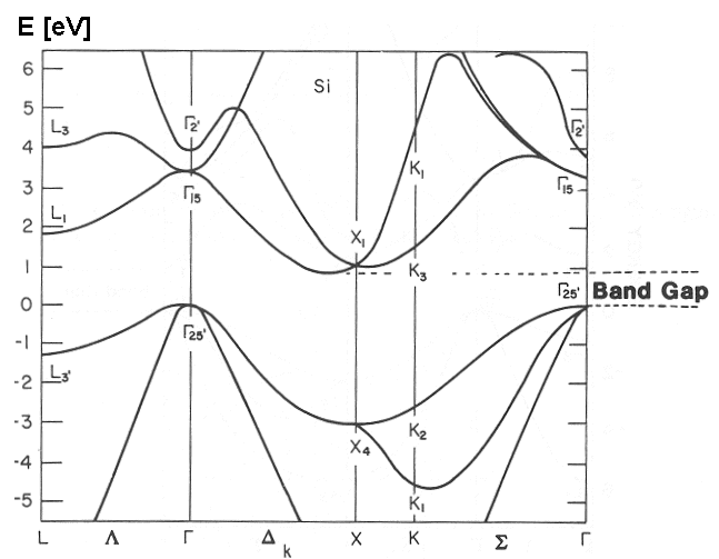
- Direct gap 3.4 eV at Gamma
- Indirect gap 1.1 eV between Gamma= (0 0 0) and a point X', close to X=(0 1 0)
Tutorial files and Tutorial structure
Follow the instructions in Tutorials#Files and download/unpack the Silicon.tar.gz.
Once the tutorial archive file is unzipped the following folder structure will appear
COPYING README Silicon/
with the Solid_Si folder containing
> ls Silicon/
PWSCF/  YAMBO/
In the Pwscf folder the student will find an input/output directory with input/output files for pw.x. The Silicon pseudopotential file is also provided.
> ls PWSCF/
convergence_scripts  input  output  psps
In the convergence_scripts you will find some useful shell scripts to run the ground state convergence runs for Silicon.
The YAMBO folder contains the Yambo input/output files and core databases.
> ls YAMBO/
2x2x2/  4x4x4/  6x6x6/  8x8x8/  Convergence_Plots_and_Scripts/  GAMMA/
The core databases are provided for several k-points grids. In addition the folder Convergence_Plots_and_Scripts contains some scripts used for the [Silicon|GW tutorial] .
Here we will just use the 8x8x8 (which is still very far from convergence) folder for computing (nonequilibrium) optical properties.
